Circuit Diagram Of Ttl Nand Gate What Is Transistor Transist
What is transistor transistor logic (ttl) circuit? Ghim trên electronics Ttl transistor nand logic
2 Input Nand Gate Circuit Diagram
Ttl nand and and gates Q4) the circuit diagram of a ttl nand gate is illustrated with a set of Looking inside a vintage soviet ttl logic integrated circuit
A 4-input ttl nand gate and its circuit symbol
[diagram] circuit diagram nand gateCircuit diagram of two input ttl nand gate Ttl circuit of not gateTtl nand and and gates.
Transistor-transistor logic (ttl)Solved for ttl nand gate circuit shown in the figure. 1 Nand gate diagramTtl nand collector logic schematic righto.

Why does the ttl family use a totem pole circuit on the output
Ttl nand gate schematicWhy does the ttl nand gate use a 4 transistor design instead of 2 ¿cómo funcionan las puertas ttl nand?What is ttl?.
3 input ttl nand gate circuitCircuit diagram of 2 input ttl nand gate Gate input ttl nand two working principleTtl nand gate circuit diagram.
![[DIAGRAM] Circuit Diagram Nand Gate - MYDIAGRAM.ONLINE](https://i2.wp.com/circuitdigest.com/sites/default/files/circuitdiagram/NAND-Gate-Circuit-Diagram.gif)
Ttl nand gate circuit diagram
Ttl logic: what is and how does it work?Ttl transistor logic nand gate input impedance output basic bjt example transistors simple inputs Nand gate circuit diagramTtl or gate circuit diagram.
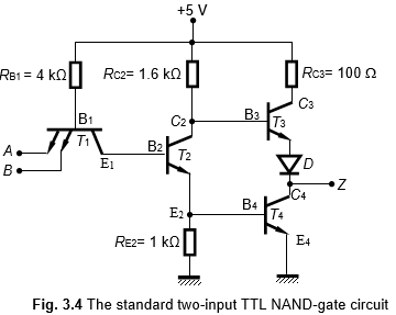
Electronic – ttl logic gate resistor values – valuable tech notesNand gate ttl My 2nd try finding the easiest way to compare two 8-bit buses. can youWorking principle of the two-input ttl nand gate ~ electronics and.

Ttl nand input gates circuit diagram gate logic states digital
2 input nand gate circuit diagramGate ttl nand collector open gates logic output Nand gate circuit diagram using diode iot wiring diagram 19152Ttl circuit: transistor -transistor logic circuit operation.
Ttl inverter diagram2 input nand gate layout .


